The recent video by David L. Jones from the EEVBlog on VFDs has inspired me to look in my junk box – I knew I had an old VFD in there. By old I mean really old – I have bought it around 1999-2000 in Munich from an electronics surplus store, along with a few other things. The module came with no documentation and there is nothing available about it online neither, so it sat in my part box for years. Until now …
The VFD in question is a module that was likely meant for a customer display of a cash register. There is a label “VFD 240W.401” on the backside of the PCB, otherwise there are no other markings apart from “VFD 240 rev 4.0” etched on the PCB (not silkscreened) and a few stickers with what are likely serial numbers.
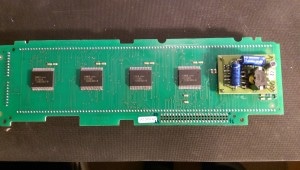
The display has two lines, 40 characters each, each character is a 5×12 matrix. The board has two connectors, one 46 pin 0.1″ spaced female header and and one 9 pin right angle header. The back side reveals 4 identical OKI MSC1162A chips and a small daughter board with an inverter circuit. The date code sticker on the inverter seems to be showing 45th week 1997 – 18 years old!
A good introduction to how a VFD works is available from Newhaven Display. However, there are a few issues that are not mentioned there. A VFD is basically a multiple triode with a directly heated cathode. Triode is a type of vacuum tube with 3 electrodes – cathode, anode (also called “plate”) and a grid. The cathode is heated by a passing current and emits electrons. Those are attracted by a positively (relative to the cathode) charged anode. In the case of a VFD, the cathode is in a form of very thin wires stretched above the segments, they can be seen glowing faintly in the dark when the VFD is powered. The anode is usually a single segment – in the case of this VFD, each anode is one square “pixel”. If the electrons emitted by the hot cathode hit the anode, they will trigger phosphorescence and the anode glows with the typical blue-green color.
The grid electrode is in the form of a thin mesh between the cathode and the anodes. It works a bit like a depletion mode MOSFET – if the voltage on the grid is the same as on the cathode, the electrons flow through it and the anodes glow. If the grid becomes more negative than the cathode, it will repel the electrons and the anodes stop glowing. The grid must never be on a higher potential than the cathode – in that case it would attract the electrons too, causing high currents to flow. Depending on the construction of the tube, it could drastically shorten its life.
Two important safety issues:
- Vacuum tubes contain vacuum. The consequence is that a VFD is a fairly fragile piece of glass, with a danger of implosion and very sharp glass shrapnel flying all over should it get accidentally broken. Handle with care!
- Vacuum tubes work with high voltages. In the case of this VFD module, the high voltage is generated by an on-board inverter and it is around 65V. That is unlikely to kill or seriously injure anyone but the zap is not pleasant. Also care should be taken with loose wires accidentally touching the exposed VFD pins – sending 65V into some unsuspecting circuitry is a sure way to fry it!
Googling “VFD 240W.401” reveals very little – only an old post on a German language forum that reveals that some other people were trying to make this module working. However, there are a few bits of important information there:
- The display is multiplexed (this is obvious from the number of pixels and the connector size)
- The multiplexing has to run all the time. If it doesn’t, the VFD will draw too much current and a tiny zener diode in the inverter will die.
- The current draw can be fairly high – 600mA and more is completely normal, if all segments are on the current can rise to 1A and more! Current limited power supply is very recommended for testing in order to prevent accidental damage to the display in case of (inevitable) mistakes. Alternatively, the blanking pin can be driven with a PWM signal with e.g. 10% duty cycle to limit the current consumption while experimenting with the module. Unfortunately, this will likely result in unwanted flicker and visual artefacts due to the PWM frequency “beating” against the refresh of the display.
In comparison to the VFD used by David L. Jones in his video, this VFD is a lot more primitive and more complicated to drive. There is no MCU that could take ASCII codes and generate the signals required for the multiplexing of the display. The datasheets for the OKI MSC1162A chips reveal that they are only 40bit shift registers with high voltage outputs designed for driving VFDs. No “smarts” here, all pixels have to be driven “manually”. The shift registers operate from 5V using TTL levels. The important pins required to drive them are:
- CL, active low, pulls the outputs low – useful for blanking and PWM brightness control
- LS, latch, transfers the data from the shift register to the output buffers
- CLK, clock input, data are read on a rising edge
- DIN, data input
- DOUT, data output
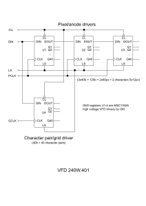
Buzzing the pins of the shift registers out with a multimeter revealed that 3 are chained together, forming a 120 bit shift register. The 4th chip is separate. The 120 bit chain drives the anodes (pixels) and the 40 bits in the second register control the grids of the characters, two characters at a time, one in the upper and one in the lower row.
The schematics reveals some complications. The DIN lines for both the “pixel” chain and the grid register are tied together, so care needs to be taken of the level on the DIN pin when advancing to next grid in order to avoid activation of the wrong character “cell” (two vertically adjacent characters sharing a common grid). The LS latch line is also common, so the same issue applies.
Buzzing out the large 46 pin connector reveals the pinout below. Some pins are repeated on the connector for unknown reasons, the pins with no labels are either not connected or have an unknown function. They are not really important to the functioning of the display, though. The smaller 9 pin connector seems to be terminated using a resistor array, but it isn’t connected to the shift registers, so its function is not known neither.
| Connector (pin 1 top left when looking from the front) | |||
| 1 | CL | 24 | |
| 2 | LS | 25 | |
| 3 | grid CLK | 26 | |
| 4 | pix CLK | 27 | GND |
| 5 | DIN | 28 | |
| 6 | 29 | ||
| 7 | CL | 30 | |
| 8 | LS | 31 | |
| 9 | grid CLK | 32 | |
| 10 | pix CLK | 33 | GND |
| 11 | DIN | 34 | |
| 12 | 35 | ||
| 13 | . | 36 | |
| 14 | Vcc (5V) | 37 | |
| 15 | GND | 38 | |
| 16 | GND | 39 | |
| 17 | 40 | ||
| 18 | 41 | ||
| 19 | 42 | ||
| 20 | Vcc (5V) | 43 | |
| 21 | GND | 44 | |
| 22 | GND | 45 | |
| 23 | 46 | ||
| R/L permanently high | |||
| CHG permanently low | |||
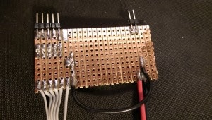
In order to hook up the display to my microcontroller board I have built a “connector” by soldering a few pins to a piece of stripboard. This fixture is better than using loose jumper wires because it ensures solid contact and avoids the need to fiddle with cables while the VFD is powered up, risking a short with potentially nasty results (there are lot of naked pins with 65V on them!). The signal lines have loops of thin wire soldered on the strips, these are used for attaching scope or logic analyzer probes.
The shift register pin mapping is a bit odd and it took me a fairly long time to work out. Each line of the character cell is 5bits (there are 5 pixels) and the bits alternate between the top and bottom character of each cell (two vertically adjacent characters). So the first 5 bits pushed into the register control a line from the top character and the next 5 bits control a line from the bottom character. The next 5 are from the top one again and so on. The data start at the bottom-most line (intended for a cursor?) and then continue from the top to bottom. The final data packet is 15 bytes (= 5x12x2 = 120bits, 120/8 = 15), sent in MSB first.
The following table shows the mapping of a pair of 5×12 characters into the 15 bytes of the data packet. The table also shows how the pixels map to a font where each character is stored as 12 bytes, with the pixels in the upper 5 bits.
| 7 | 6 | 5 | 4 | 3 | 2 | 1 | 0 | |
| 0 | B1.5-1 | |||||||
| 1 | B2.3-0 | B3.7 | ||||||
| 2 | B3.1-0 | B4.7-5 | ||||||
| 3 | B5.7-3 | |||||||
| 4 | B6.5-1 | |||||||
| 5 | B7.3-0 | B8.7 | ||||||
| 6 | B8.1-0 | B9.7-5 | ||||||
| 7 | B10.7-3 | |||||||
| 8 | B11.5-1 | |||||||
| 9 | B12.3-0 | B13.7 | ||||||
| 10 | B13.1-0 | B14.7-5 | ||||||
| 11 | B0.7-3 | |||||||
| 7 | 6 | 5 | 4 | 3 | 2 | 1 | 0 | |
| 7 | 6 | 5 | 4 | 3 | 2 | 1 | 0 | |
| 0 | B1.0 | B2.7-4 | ||||||
| 1 | B3.6-2 | |||||||
| 2 | B4.4-0 | |||||||
| 3 | B5.2-0 | B6.7-6 | ||||||
| 4 | B6.0 | B7.7-4 | ||||||
| 5 | B8.6-2 | |||||||
| 6 | B9.4-0 | |||||||
| 7 | B10.2-0 | B11.7-6 | ||||||
| 8 | B11.0 | B12.7-4 | ||||||
| 9 | B13.6-2 | |||||||
| 10 | B14.4-0 | |||||||
| 11 | B0.2-0 | B1.7-6 | ||||||
| resulting packet is 15 bytes | ||||||||
| B X.Y-Z = Byte X, bits Y to Z | ||||||||
| Send MSB first | ||||||||
In order to quickly test the driving of this display from a microcontroller I have used an Arduino NG board to prototype a simple example. Controlling this VFD is fairly CPU intensive because it has to be constantly fed with quite a lot of data in order to achieve decent refresh rate without flicker. The shift registers are able to work up 4MHz for a good reason! The minimal 30Hz refresh rate requires: 40x15x30 = 18000 bytes/second, that gives 144kbps sustained transfer rate as a minimum, counting with probably at least double to achieve 60Hz is a good idea.
The sample code implements two techniques how to drive the display, switchable at compile time using some #ifdef macros. One bitbangs the individual lines of each character, working in 5bit blocks. This works, but it requires a lot of CPU time. The advantage is that it results in smaller, more readable code.
The second version uses the SPI peripheral. Because SPI on AVR can work only in 8 or 16 bit words, it is necessary to pre-pack the character bits into a buffer and then transfer that at once. This is faster, in case of using interrupts (not implemented in the example) it would give a chance for the MCU to do something else while the display is being refreshed. The disadvantage is a large pile of bit shifting and mangling code that is hard to read and takes a lot of memory.
The code was tested on both Arduino NG (ATMega168 @ 16MHz) and Arduino Mega 2560. In both cases it is necessary to change from using digitalWrite() function to direct register access, especially for the bitbanging code, otherwise the code is way too slow to achieve a decent, flicker-free refresh rate.
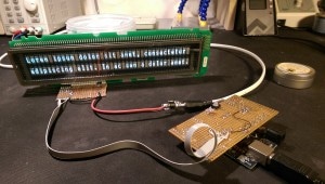
This is how the VFD looks running the demo program:
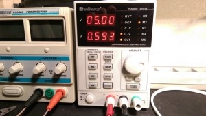
And the current being drawn by the display alone (the Arduino is powered from USB) – that’s 600mA right there!
All in all, it was an interesting learning experience.The VFD looks great, unfortunately its high current consumption, relative fragility and complicated driving make it not very easy to use. In order for this module to be really useful it will likely be necessary to implement a dedicated controller, offloading the display handling from the main application processor. Probably some sort of “backpack” emulating the functionality of the popular HD44780 controller could work nicely. More modern VFD modules from Noritake took exactly this approach, providing a drop-in replacement for the popular character LCD modules.
Finally, the information here is provided as-is, with no guarantee of correctness. I did work for me and I hope that this information will prove useful to someone, but don’t blame me if your module doesn’t work or the magic smoke escapes.
Resources
- Arduino example: vfd240.zip
- The 5×12 font used is modified from: https://github.com/idispatch/raster-fonts/blob/master/font-5×12.c I believe that it is OK to use, but in case of doubt contact the author of that project.
- OKI MSC1162A datasheet




Brilliant! thanks for sharing this. I got the very same display, back in 2012, also in Munich. Will try this out! Bravo!
Cool, I am glad that this is useful for someone.
Good luck with the hacking! And if you manage to write simpler code for running this using SPI (or some other peripheral), I am all ears. The current code is a pain 🙁
Brilliant article, thank you! Do you happen to know the voltage of the Zener? I think I killed mine … thanks 🙂
Hello,
According to the German article linked in the text it is 9.1V. They say it is ZPD9.1 but that one doesn’t seem to be available in SOT23. The diode on my board has “Y1” marking, that is more likely to be something like BZX84C11-V or similar with a 11V Zener voltage.
However, any similarly rated Zener in a matching package would likely do (cathode is towards the center of the board, anode towards the right), the diode is only there to ensure that the filaments have positive voltage relative to ground by a few volts, otherwise it wouldn’t be possible to turn the segments off completely by grounding the grids.
BTW, it is the SOT23 diode on the right next to the 3 caps and a resistor on the main board, just under the inverter.
Thanx, I will try to fix it this weekend 🙂
Cool, good luck!
Inspiring! Keep the great job.
Thanks!
Hey! Thanks for your brilliant (reverse) engineering!
I’ve got a question: I wrapped your code into a library, fixed some things and made it very easy to use, is it ok for you if I publish it on Github under GNU LGPL? Maybe it can be useful for someone.
Hi Julian,
By all means, do so. If you manage to get something online, let me know and I will link to it from the article as well.
I didn’t make a library out of it at the time because I didn’t like how the code worked. It did get the job done but required either bitbanging or a lot of bit twiddling and memory to prepare the buffers for the SPI. Not really easy to integrate.
I could imagine this would be a breeze to drive with the PIO peripherals on RP20240 and similar these days but with a classic ATMega it was a pain.
Jan
Hello 🙂
Do you still have the library?
If you already put it on GitHub, what is it called?
Thanks in advance 🙂
Hello,
There is no library. The example code is attached to the post.
Jan
I know that, this question was to the other user 🙂
I mean the user Julian, because a library would be really useful.
Thanks for reverse engineering the display, i ordered one a few days ago,
i will try it when it arrives 😉
I managed to modify it (with help of ChatGPT) to display everything that gets sent through UART Serial to the arduino.
If someone wants it: https://www.mediafire.com/file/ddi9db0pmsv9k5f/VFD240driver.zip/file
Hey!
Thx for the work. It helped a lot.
Is the arduino example still available? I don’t seem to be able to download it.
Tobias
The example is available as it were always was on the website.